Optical Design and Thin Film Coating Facility
Our facility is capable of optical design, optical manufacturing, infrared thin film coating, diamond like carbon (DLC) coating and metrology.

In addition to R&D activities and consultancy needed by the optics industry, mass production is carried out with our industry standard infrastructure.

Our capabilities are as follows.

ISO 7 Clean Room System
• 120 m2 class 10000 cleanroom
• 200 m2 machine room
• Compressed air, nitrogen generator, sandblaster, chiller, ultra pure water systems and wet & flow benches
Optical Design
Optical Design
Design of Optical Systems and Components
• Zemax OpticStudio design software
• Lenses, mirrors, prisms and freeform surfaces
• Zoom lens, objectives and complex systems
• Opto-mechanic design

Optical Thin Film Design
• Optilayer Thin Film Design Software
• Anti-reflective coatings
• Mirror surfaces
• All kinds of filter coatings
• Beamsplitter surfaces
• Polarizers and color coatings
Optical Manufacturing
Single Point Diamond Turning
• Precitech Nanoform X SPDT Lathe
• Upto 440mm dimamter machining
• Spherical, aspherical, diffractive, conical, fresnel, prism and free-form optical surfaces
• Virtual/augmented reality, LIDAR/remote sensing
• Spectrograph/hyperspectral imaging, Medical imaging
• Portable consumer optoelectronic devices
• Optical components including the optics of cameras, x-ray, lasers, solar cells and mobile phones
• Injection molding, replication and electroforming
• Processing plastics, glass and crystals, metals, alloys and metal coatings
Optical Thin Film Coating
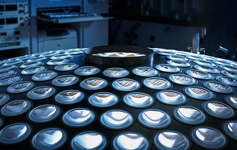
• Thin film coating and product development in regions (VIS, NIR, SWIR, MWIR, LWIR)
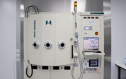
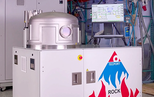
• Hanil Vacuum 900DA PVD system
• 900 mm chamber size
• 10-7 Torr High Vacuum Pumping
• Chamber temperature up to 300 degrees
• Dome type rotation system for substartes
• Electron Beam, Ion Beam and Resistance heat sources
• Tavg > 98% - Ravg < 0.4% @ 3.6–4.9μm
on Ge, Si,&-CaF2 substrates

In the defense industry
• Forward Looking Infrared (FLIR) used in military vehicles (fighter jets, drones, etc.) and equipment
• Thermal scanner warhead (heat-seeking) system
• Night and thermal vision camera applications

Other industrial applications
• Safety technology; filters for gas analysis, mining, alcohol measurement, building technology
• Environmental technology; biogas analysis, greenhouse gas analysis, emission monitoring
• Medical technology; patient and anesthesia monitoring
• Agriculture; biogas plants, quality control
• Flame detection; pyroelectric detectors
• Infrared spectroscopy; chemical analysis, e.g. alcohol, sugar and water content

Hard Carbon DLC Coating
• Functional coatings DLC (diaomond like carbon) compatible with military standards
• DLC integrated Multilayer Coating
• Uniformity < +/- 2.5%
• Raverage < 4% @ 3.4 – 4.6um, DLC Si
• Raverage < 4% @8 – 12um, DLC Ge
• RF Plasma with Auto Matching
• Substrate holder up to 585mm in diameter
• High resistivity multispectral optical coatings
• Durable and stable operation of optics
• Other areas of use: Engine parts and injectors, Aviation fasteners and components, Industrial machine components, Aluminum and non-ferrous metal forming, Plastic injection molding tools, Medical instruments, Cutting tools, Hard chrome replacement, Semiconductor technology, Watches and jewelry
Non-Contact 3D Optical Profilometer
• Step height measurement
• Surface topography
• Measurement of surface roughness parameters
• Imaging of nano and micro structures
Contact Stylus Profilometer
• Measurement of surface quality and shape
• Surface finish and form measurement
• Spherical/Aspherical and freeform surface analysis
• 300 mm single track measurement
FTIR Spectroscopy
FTIR Spectroscopy
• Analysis of thin films and coatings
• 2 - 25 micrometer bandwidth optical reflectance and transmittance measurements
Laser Interferometer
• Surface shape error
• Transmitted wavefront measurement
 

google maps embedded map